
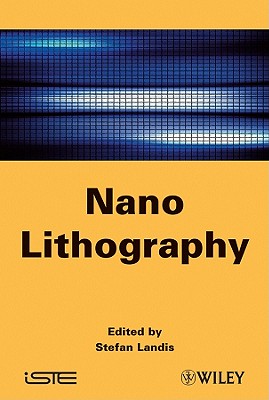
Nano–lithography
Book Details
Format
Hardback
ISBN-10
1848212119
ISBN-13
9781848212114
Publisher
ISTE Ltd and John Wiley & Sons Inc
Imprint
ISTE Ltd and John Wiley & Sons Inc
Country of Manufacture
GB
Country of Publication
GB
Publication Date
Jan 14th, 2011
Print length
320 Pages
Weight
635 grams
Dimensions
23.60 x 16.00 x 2.50 cms
Product Classification:
Circuits & componentsElectronics: circuits and components
KSh 25,000.00
Currently unavailable
0 in stock
Delivery Location
Delivery fee: Select location
Secure
Quality
Fast
Lithography is a complex tool based on the concept of imprinting an original template version onto mass output originally using relatively simple optical exposure, masking, and etching techniques, and now includes exposure to X-rays, high energy UV light, and electron beams in processes developed to manufacture everyday products.
Lithography is an extremely complex tool – based on the concept of “imprinting” an original template version onto mass output – originally using relatively simple optical exposure, masking, and etching techniques, and now extended to include exposure to X-rays, high energy UV light, and electron beams – in processes developed to manufacture everyday products including those in the realms of consumer electronics, telecommunications, entertainment, and transportation, to name but a few. In the last few years, researchers and engineers have pushed the envelope of fields including optics, physics, chemistry, mechanics and fluidics, and are now developing the nanoworld with new tools and technologies. Beyond the scientific challenges that are endemic in this miniaturization race, next generation lithography techniques are essential for creating new devices, new functionalities and exploring new application fields. Nanolithography is the branch of nanotechnology concerned with the study and application of fabricating nanometer-scale structures - meaning the creation of patterns with at least one lateral dimension between the size of an individual atom and approximately 100 nm. It is used in the fabrication of leading-edge semiconductor integrated circuits (nanocircuitry) or nanoelectromechanical systems (NEMS). This book addresses physical principles as well as the scientific and technical challenges of nanolithography, covering X-ray and NanoImprint lithography, as well as techniques using scanning probe microscopy and the optical properties of metal nanostructures, patterning with block copolymers, and metrology for lithography. It is written for engineers or researchers new to the field, and will help readers to expand their knowledge of technologies that are constantly evolving.
Get Nano–lithography by Stefan Landis at the best price and quality guaranteed only at Werezi Africa's largest book ecommerce store. The book was published by ISTE Ltd and John Wiley & Sons Inc and it has 320 pages.
Customers Who Bought This Also Bought

Introduction To Electronic Circuits: A Design-oriented Approach
KSh 9,900.00

Intelligent Techniques for Security of Medical Data
KSh 22,500.00

Hardware Supply Chain Security
KSh 19,800.00
Cryptographic Engineering
KSh 39,600.00

Functional Design Errors in Digital Circuits
KSh 23,400.00

Viruses, Hardware and Software Trojans
KSh 23,400.00
mm-Wave Silicon Technology
KSh 36,000.00

Electrical Engineering Experiments
KSh 8,000.00

In-Memory Computing
KSh 16,200.00

Protection Principle and Technology of the VSC-Based DC Grid
KSh 21,600.00

Languages, Design Methods, and Tools for Electronic System Design
KSh 8,100.00
Soft Error Reliability of VLSI Circuits
KSh 8,100.00
More in This Genre
Introduction To Electronic Circuits: A Design-oriented Approach
KSh 9,900.00
Intelligent Techniques for Security of Medical Data
KSh 22,500.00
Hardware Supply Chain Security
KSh 19,800.00
Cryptographic Engineering
KSh 39,600.00
Functional Design Errors in Digital Circuits
KSh 23,400.00
Viruses, Hardware and Software Trojans
KSh 23,400.00