

Book Details
Format
Paperback / softback
ISBN-10
1447110625
ISBN-13
9781447110620
Edition
Softcover reprint of the original 1st ed. 2001
Publisher
Springer London Ltd
Imprint
Springer London Ltd
Country of Manufacture
GB
Country of Publication
GB
Publication Date
Aug 30th, 2012
Print length
346 Pages
Weight
522 grams
Dimensions
23.40 x 15.70 x 1.90 cms
Product Classification:
Industrial chemistryIndustrial chemistry and chemical engineeringIndustrial chemistry and chemical engineeringChemical engineeringMechanical engineeringMaterials scienceProduction and industrial engineeringProduction engineeringElectronics engineeringOther technologies & applied sciencesOther technologies and applied sciences
KSh 32,400.00
Currently unavailable
0 in stock
Delivery Location
Delivery fee: Select location
Secure
Quality
Fast
In the 50 years since the invention of transistor, silicon integrated circuit (IC) technology has made astonishing advances. In state of the art silicon Ie manufacturing process, plasma is used in more than 20 different critical steps.
In the 50 years since the invention of transistor, silicon integrated circuit (IC) technology has made astonishing advances. A key factor that makes these advances possible is the ability to have precise control on material properties and physical dimensions. The introduction of plasma processing in pattern transfer and in thin film deposition is a critical enabling advance among other things. In state of the art silicon Ie manufacturing process, plasma is used in more than 20 different critical steps. Plasma is sometimes called the fourth state of matter (other than gas, liquid and solid). It is a mixture of ions (positive and negative), electrons and neutrals in a quasi-neutral gaseous steady state very far from equilibrium, sustained by an energy source that balances the loss of charged particles. It is a very harsh environment for the delicate ICs. Highly energetic particles such as ions, electrons and photons bombard the surface of the wafer continuously. These bombardments can cause all kinds of damage to the silicon devices that make up the integrated circuits.
Get Plasma Charging Damage by Kin P. Cheung at the best price and quality guaranteed only at Werezi Africa's largest book ecommerce store. The book was published by Springer London Ltd and it has 346 pages.
Customers Who Bought This Also Bought

Thermomechanical Pulp
KSh 16,750.00

Cleaning
KSh 30,950.00

Industrial Chemical Thesaurus, 2 Volume Set
KSh 100,450.00

Translational Chemical Ecology
KSh 22,500.00

Biocatalysis and Biotransformations
KSh 13,950.00

Cleaning
KSh 7,200.00

Biomolecules
KSh 12,350.00

Chemical Engineering: 25 Must-Know Process Design Principles
KSh 11,500.00

Design and Simulation of Conventional and Complex Distillation Systems
KSh 21,250.00

Semiconducting Fibers
KSh 10,100.00
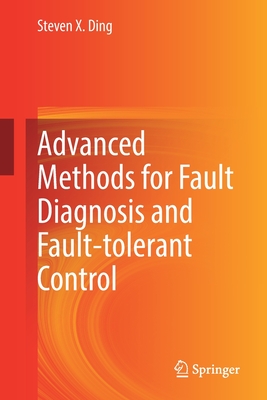
Advanced methods for fault diagnosis and fault-tolerant control
KSh 21,600.00
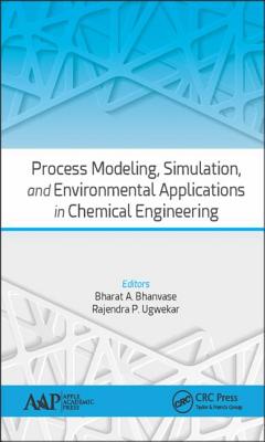
Process Modeling, Simulation, and Environmental Applications in Chemical Engineering
KSh 19,800.00